
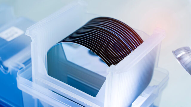
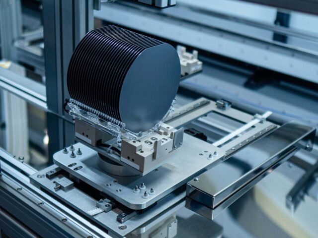
Patterned wafers are an essential component in many modern technologies. They are used in a wide range of industries, from microelectronics to renewable energy.
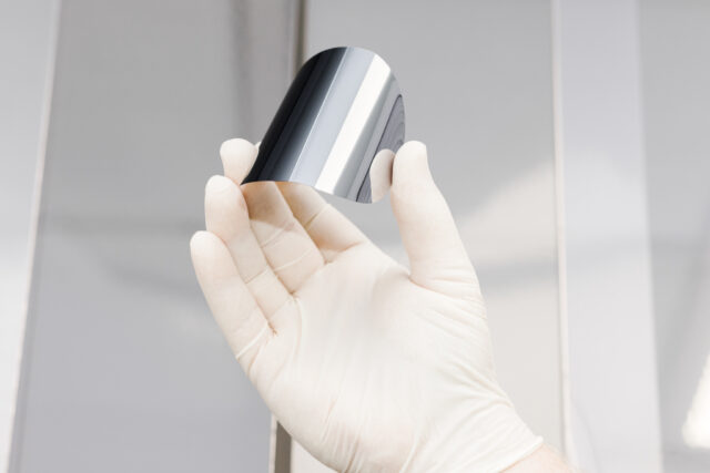
A patterned wafer is a flat, disc-shaped material, typically made of silicon or another semiconductor material, which has been coated with a thin layer of a material such as an oxide or nitride. This layer is then patterned using lithography techniques to create the desired circuit or structure on the surface.
The manufacturing process involves several stages, each of which is critical to producing high-quality wafers. This article provides an overview of the manufacturing process and applications.
Stage 1: Wafer Preparation
Wafer preparation is the first stage in the manufacturing process. This stage involves preparing the silicon for further processing by cleaning it and depositing a thin layer of oxide or nitride onto the surface. The quality of this initial preparation stage is critical to the success of the subsequent stages of the manufacturing process.
Cleaning
The first step is cleaning. It is thoroughly cleaned to remove any contaminants and defects from the surface. The cleaning process can involve several steps, such as rinsing the wafer in deionized water, immersing it in a chemical bath, and using a plasma cleaning process to remove any remaining impurities.
Oxide or Nitride Deposition
After cleaning, a thin layer of oxide or nitride is deposited onto the surface. This layer acts as a protective coating during subsequent processing steps. The thickness of the oxide or nitride layer can vary depending on the application.
The oxide or nitride layer is deposited using a variety of methods, including chemical vapor deposition (CVD), physical vapor deposition (PVD), and thermal oxidation. CVD involves the reaction of gaseous precursors to form a solid coating on the wafer surface.
PVD involves the deposition of a thin film of oxide or nitride onto the wafer surface using a vacuum chamber. Thermal oxidation involves exposing the wafer to high temperatures in the presence of oxygen to form an oxide layer.
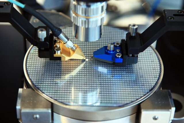
Stage 2: Lithography
The next stage in the manufacturing process is lithography. This involves patterning the wafer surface with the desired circuit or structure using photolithography. It is coated with a photoresist, which is a light-sensitive material that hardens when exposed to light.
A patterned mask is then placed over it, and light is directed onto the wafer through the mask. The exposed areas of the photoresist harden, and the unexposed areas remain soft.
The wafer is then washed with a developer solution that removes the soft, unexposed areas of the photoresist. The remaining photoresist acts as a mask, protecting the underlying layer of oxide or nitride during subsequent processing steps.
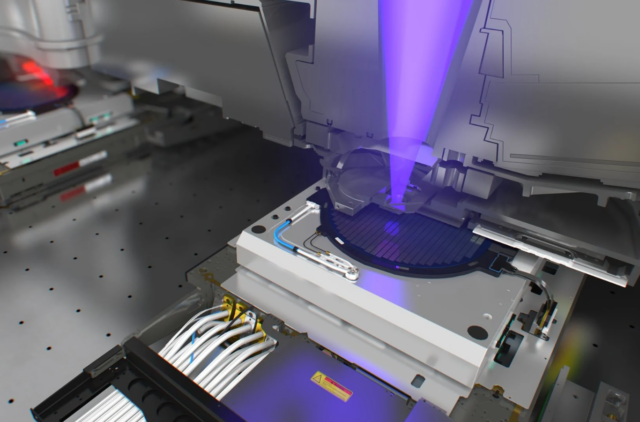
Stage 3: Etching
Etching is the third stage in the manufacturing process of patterned wafers. This stage involves selectively removing the unprotected areas of the oxide or nitride layer to create the desired pattern on the surface.
The etching process is critical to producing high-quality patterned wafers, as it determines the accuracy of the pattern and the quality of the final product.
Wet Etching
There are two primary methods of etching used in the manufacturing process of patterned wafers: wet etching and dry etching. Wet etching involves exposing it to a chemical solution that selectively dissolves the unprotected areas of the oxide or nitride layer.
This method is relatively inexpensive and can produce high-quality patterns. However, it is a slow process and can result in uneven etching.
Dry Etching
Dry etching is a faster and more precise method of etching. It involves using a plasma to selectively remove the unprotected areas of the oxide or nitride layer. This method is commonly used in the microelectronics industry, as it can produce very precise patterns with high accuracy. However, it is a more expensive process than wet etching.
Masking
During the etching process, the photoresist mask that was applied during the lithography stage protects the underlying layer of oxide or nitride. Once the etching process is complete, the photoresist mask is removed using a solvent. The resulting pattern on the surface is then ready for further processing, such as doping.
Stage 4: Doping
The final stage in the manufacturing process is doping. Doping involves adding impurities to the semiconductor material to change its electrical properties.
This is done by exposing the it to a dopant material, such as boron or phosphorus, in a high-temperature furnace. The dopant atoms diffuse into the semiconductor material and alter its electrical conductivity.
Applications of Patterned Wafers
Patterned wafers are a critical component in a wide range of modern technologies, and their applications are constantly expanding.
They are commonly used in the microelectronics, solar energy, and sensor industries, among others. In this article, we will explore the various applications in detail.
Microelectronics
The microelectronics industry is one of the largest consumers. The intricate circuits and structures that makeup computer chips and other electronic devices are created using them.
The small size of the transistors and circuits on them enables the creation of smaller, faster, and more powerful devices.
Solar Cells
They are used in the production of solar cells. The gridlines that collect and transport electrical current are created by patterning the surface. The creation with high efficiency and low cost is critical to the widespread adoption of solar energy.
Sensors
Patterned wafers are used to create the sensing elements in sensors. These sensors detect changes in temperature, pressure, or other physical properties. They are used in a wide range of industries, from automotive to aerospace.
Medical devices
They are also used in the medical device industry. They are used to create sensors and other components in medical devices such as pacemakers, defibrillators, and glucose monitors. These devices require high levels of precision and reliability, and patterned wafers play a critical role in their production.
Conclusion
Patterned wafers are a crucial component in many modern technologies. The manufacturing process involves several stages, including wafer preparation, lithography, etching, and doping. Each stage is critical to producing high-quality wafers.
Patterned wafers are used in a wide range of applications, including microelectronics, solar cells, and sensors, and their importance in modern technology is only expected to increase in the years to come.


